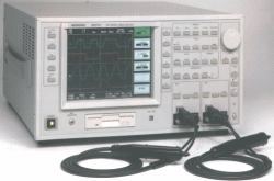
MDS750 EO Digital Oscilloscope
A NEW EASY-TO-USE 10GHz-OSCILLOSCOPE USING EO-SAMPLING

Combining Photonics and Electronics
A microwave, multi-gigabit digital oscilloscope using a new technology —electro-optic (EO) sampling— has made its debut. The combination of photonics and electronics makes this oscilloscope easier-to-use than conventional digital oscilloscopes and has enabled measurement of 10-GHz broad-band signals.
Laser pulse-based sampling
The electric field produced by the signal voltage in the
measured circuit varies the birefringent properties of an EO crystal, which acts
to vary the polarization state of a laser pulse passed through the EO crystal.
The signal waveform can be then monitored by measuring the change in the
polarization of this laser pulse. In special cases, a picosecond laser pulse is
used as a sampling pulse, meaning that EO sampling technology makes possible
measurements on the order of 100GHz. This most recently developed EO sampling
oscilloscope uses a laser pulse of less than 30 picoseconds, and thus can
measure 10-GHz signal waveforms.
Four
Major EO Sampling Features
Features1One point contact measurement
Conventional electronic probes require a ground wire. In such a setup, the fact that the ground plane is a non-perfect conductor causes a common-mode voltage to appear, meaning that the measured waveform will be affected by the ground point. In contrast, since the EO handy probe measures the intensity of the electric field produced by the signal line, it needs no ground wire.
Common mode voltages VC1, VC2, VC3 |
Compared with the waveform produced by the MDS750, the detected waveform of a conventional FET probe is noisy for the common mode voltage in the ground wire.
|
EO handy probe
|
Conventional electronic probe
|
|
MDS750 |
FET probe |
Features2Ultra-high input impedance
A conventional broadband oscilloscope and sampling oscilloscope have an input impedance of 50ohms. This relatively low input impedance affects the device under test (DUT). FET probes have a higher input impedance (100kohm / / 0.4pF), but not high enough. In contrast, the EDS 1100 EO handy probe has a virtually infinite input impedance, since the EO crystal acts as an insulator. Its input resistance is more than 100Mohm and its input capacitance is less than 0.2pF. This means that EO handy probes have virtually no affection on the measured circuits.
|
Input equivalent circuit of an EO handy probe |
Features310-GHz broadband measurement
With their high input impedance, FET probes have conventionally been used to perform broadband measurements. However, this EO handy probe has a much higher input impedance than that of any FET probe. MDS750 has a 10-GHz cutoff frequency—four times higher than that of an FET probe.
Features4Safe, very high input voltage
The distance between the metal tip and the photo-detector is a few centimeters. Since this gap naturally acts as an insulator, it gives the MDS750 an input damage level of more than 1000V. For an input voltage on the order of only tens of volts, FET probes and conventional sampling oscilloscope must be handled very carefully. The EO handy probe can be used safely without taking special precautions.
Operational "Feeling" of a Conventional Digital Oscilloscope
No longer does EO sampling mean having to learn difficult and special operations. The MDS750 boasts of easy-to-use operation by providing the operational feeling of a conventional digital oscilloscope.
Large 8.4-inch color liquid crystal display
The MDS750 is equipped with a large, easy-to-view 640 (W)
× 480 (H) -dot, 8.4-inch TFT color liquid crystal display. It can display up to
four traces (two current waveform traces and two load waveform traces).
Waveform, cursor, scaling and other indicator colors can be freely selected to
suit your liking. A backlight is normally lit for easier viewing.
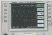
Delay Functions
Applying a delay allows you to more easily observe the portion of the waveform which you wish to view. For example, set the delay to 63.8ns if you wish to more closely view the section indicted by the red-framed box at right. You can apply delay times ranging from 130ns for a fast sweep range and 1.1µs for a slow sweep range. For even greater utility, use this function together with the trigger function to get a more detailed view of the desired section.

Trigger Function
Triggering can be caused with an externally supplied 10-MHz to 2-GHz frequency signal. Internally, the frequency is divided at the appropriate frequency and then supplied to the trigger circuit. Like ordinary oscilloscopes, trigger level (-2V to +2V), slope (rise, fall) and coupling (DC, AC) can be set.

Zoom Function
Current waveforms can be expanded along the voltage axis by 1, 2, 5, 10, 20, 50, or 100 times, and along the horizontal axis by 1, 2, 5, or 10 times. Load waveforms can be also expanded independently. Their magnifications along both of the vertical and horizontal axes are the same zooming rate as the current waveforms. Since magnification is performed based on averaged data, the vertical axis resolution of the screen is not reduced at all.
Footswitch-activated RUN / STOP functions
Use of the optional footswitch allows the RUN and STOP to be operated by foot, freeing both hands and greatly facilitating waveform measurement. With connecting an ON / OFF contact switch to the EXT RUN / STOP port on the front panel instead of the footswitch, the remote control is available.

High-speed averaging function
The MDS750 is equipped with an averaging circuit that display results with almost real-time feeling. The sampling time is roughly the sampling period x 1100 / number of times. Since, for fairly fast trigger frequencies and sweep ranges, the sampling period is roughly 1µs, measurement requires only about 1.1sec even when the averaging number is set to 1024. The averaging number can be set to between 1 and 16384 in powers of 2. Averaging progress is indicated with an analog bar graph.
|
Averaging number : 1 |
Averaging number : 1024 |
Waveform saving
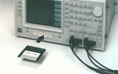
![]() To floppy disk
To floppy disk
The MSD750 is equipped with a 3.5-inch floppy disk drive-greatly facilitating the saving and arrangement of data. Load waveforms are displayed on the MDS750 screen. The disk drive supports MS-DOS-formatted 720kB and 1.44MB floppy disks.
![]() To internal RAM
To internal RAM
Up to 99 waveforms can be saved to the MDS750 's built-in memory. A backup battery for internal memory power means that the data won 't be lost in case of power off. Up to two saved waveforms can be display at the same time.
Cursor measurement
Cursors can be used to measure the voltage ( △V ) and time( △T )
of waveforms displayed on the screen. Since the ( △V ) and ( △T )
measurement modes can be independently activated and deactivated, you can measure either one or another, or measure both at the same time, giving you more flexibility. The measured value is the voltage or time between cursor 1 and cursor 2, and it is displayed with a precision of 4 digits.

Hard copies
GP-IB type plotters can output a hard copy of the screen information. To use, connect the plotter to the GP-IB port on the MDS750 's rear panel.
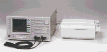
EO Digital Oscilloscope Applications
"Measuring the signal is very difficult when observing waveforms of microwave circuits or ultra high speed digital circuits", "Even if measuring it is done, the condition of the circuit is disturbed at the moment" or "Waveform changes due to the location of ground point". The digital oscilloscope by which those troubles are solved was developed. Moreover, since it also offers 1000V input damage level, it can be treated easily against conventional microwave instruments.
Measuring I / O signal waveforms of a GaAs IC
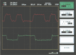
A test circuit for measuring I / O signals of a GaAs IC-fabricated D-type flip-flop is shown below. The clock input to the flip-flop is 2.0 Gbps (NRZ), and the input signal pattern is [01010011]. Channel 1 and 2 probes are brought into contact with the input and output lines, respectively.
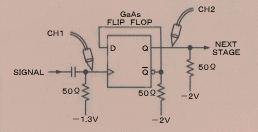
The measured input and output waveforms are shown below. With the test circuit mounted on a 50-ohm microstrip line hybrid printed circuit board, the probes do not disturb the circuit, making for ease-of-measurement. These waveforms are the results of 1024-time averaging.
Measuring sampling gate pulses
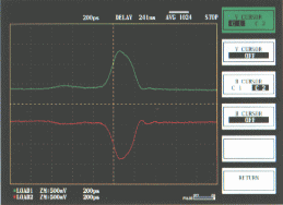
A well-known sampling gate circuit is shown below. The channel 1 probe is brought into contact with one of the diode gates and the channel 2 probe with another. The diode gate pulses must have an inverted symmetrical pulse shape. If asymmetrical, the difference from symmetry causes a measurement error due to charging the capacitance C.
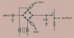
The measured gate pulse waveforms are shown below. Using a conventional FET probe, it is very difficult to accurately measure the signal in such circuit without disturbing it, since the ground point changes the waveforms.
Specifications
| Vertical system | |
| Input channels | CH1 and CH2 |
| Input CR | more than 100Mohm / / less than 0.2pF (at probe tip) |
| Input sensitivity | 5mV / div to 2V / div, 9ranges with 1-2-5steps |
|
Accuracy |
less than ± 3% at 1MHz and full scale |
| Bandwidth | 10GHz (-3dB) |
| Rise time | less than about 35ps |
| Overshoot | less than 5% |
| Vertical mode | CH1, CH2, CH1 and CH2 |
| Zoom | 1 to 100 times, 7 ranges with 1-2-5steps |
| Input voltage | less than 20 div (± 10 div) |
| Channel isolation | more than 60dB at 1GHz |
| Input damage level | more than ± 1000V (DC + AC peak) at probe tip |
| Horizontal system | |||||||||||||||||||||||||||||
| System | Sequential sampling method | ||||||||||||||||||||||||||||
| Sweep time | 10ps / div to 0.1µs / div, 13ranges will 1-2-5steps | ||||||||||||||||||||||||||||
| Accuracy | less than ± 3% for full scale (10ps / div to 0.1ns / div) | ||||||||||||||||||||||||||||
| less than ± 1.5% for full scale (0.2ns / div to 0.1µs / div) | |||||||||||||||||||||||||||||
| Sweep mode | Signal and Continuous | ||||||||||||||||||||||||||||
| Zoom | 1, 2, 5, 10times | ||||||||||||||||||||||||||||
Sweep delay
|
|||||||||||||||||||||||||||||
| MD indicates minimum delay time | |||||||||||||||||||||||||||||
| Minimum delay time | 60ns max at 10ps / div | ||||||||||||||||||||||||||||
| Sampling frequency | approx. 1MHz max | ||||||||||||||||||||||||||||
| Jitter | less than 10psrms at 0ns delay time | ||||||||||||||||||||||||||||
| Trigger system | |
| Source | External |
| Mode | NORM |
| Coupling | DC, AC |
| Slope | Rise or Fall |
| Input resistance | 50ohm |
| Frequency range | 10MHz to 2GHz |
| Sensitivity | -3 to +10dBm (10 to 500MHz) |
| 0 to +10dBm (0,5 to 1GHz) | |
| +3 to +10dBm (1 to 2GHz) | |
| Trigger level range | -2V to +2V |
| Input damage level | less than 3Vrms max or 10Vp-p max |
| Input connector | SMA |
| Signal processing system | ||||||||||||||
| Filter | Low-pass filter (LPF) and high-pass filter (HPF) | |||||||||||||
|
Characteristics |
|
|||||||||||||
| Averaging function | ||||||||||||||
| System | Simple addition method | |||||||||||||
| Averaging number | 2n (n = integer from 0 to 14) | |||||||||||||
| Speed | approx. sampling period × 1100 / time | |||||||||||||
| A / D converter | 22bits × 1024words | |||||||||||||
| Memory | 1000words are displayed in 1024words | |||||||||||||
| Output signals | ||
| Output | CH1 and CH2 | |
| Output impedance | approx. 500ohm | |
| Output voltage | approx. 40mV / full scale at 2 V / div | |
| Calibration signal | ||
| Waveform | Sine wave | |
| Frequency | 100MHz ± 0.1% | |
| Amplitude | 600mVp-p ± 1% | |
| Output terminal | 50-ohm microstrip line | |
| Advanced functions | ||
| Save | 99 waveforms | |
| Recall | 2 waveforms | |
| Vertical Zoom | 1 to 100times at 7ranges with 1-2-5steps | |
| Horizontal Zoom | 1, 2, 5, 10times | |
| Vertical position | Adjustable | |
| Horizontal position | Adjustable | |
| Cursor measurements |
Readout in |
|
| Display digits | 4digits | |
| Plot | Output to GP-IB type plotter | |
| RUN / Stop Function | Key, GP-IB, or external foot switch | |
| Floppy disk | |
| Driver | A 3.5-inch FDD |
| FD | 720kB or 1.44MB |
| Format | MS-DOS |
| Display system | |
| Monitor | 8.4-inch color liquid crystal display |
| Resolution | 640 (W) × 480 (H) dots |
| Backlight | Always ON |
| No. of display waveforms | 4 waveforms (2 current and 2 load waveforms) |
| Communications | |
| Communications Form | GB-IP |
| Commands | Writing and readout of parameters and waveforms |
| Probe | |
| Weight | Pen-type probe of approx. 80g with cables of approx. 240g |
| Dimensions | 150mm (L) × 27mmØ (maximum diameter) |
| Tip is less than 1mmØ | |
| General | |
| Operating temperature | 0 to 40ºC (Guaranteed at 23 ± 10ºC) |
| Operating humidity | 40ºC / less than 90% RH (Guaranteed at 33ºC / less than 80% RH) |
| Storage temperature | -10 To 60ºC, 60ºC / less than 80% RH |
| Power supply | 100V, 117V, 217V, 234V, AC ± 10% |
| Power consumption | approx. 110VA at 100V AC |
| Dimensions | 430 (W) × 220 (H) × 500 (D) mm (excluding projection) |
| Weight | approx. 20kg |
| Standard accessories |
EO handy probe (EP01) |
(1pc) |
| Optional |
EO handy probe (EP01) |
![]() MICRONIX Corporation reserves the right to make changes in
design, specification and other information without prior notice.
MICRONIX Corporation reserves the right to make changes in
design, specification and other information without prior notice.
Products list | brand | Model No. | Home